
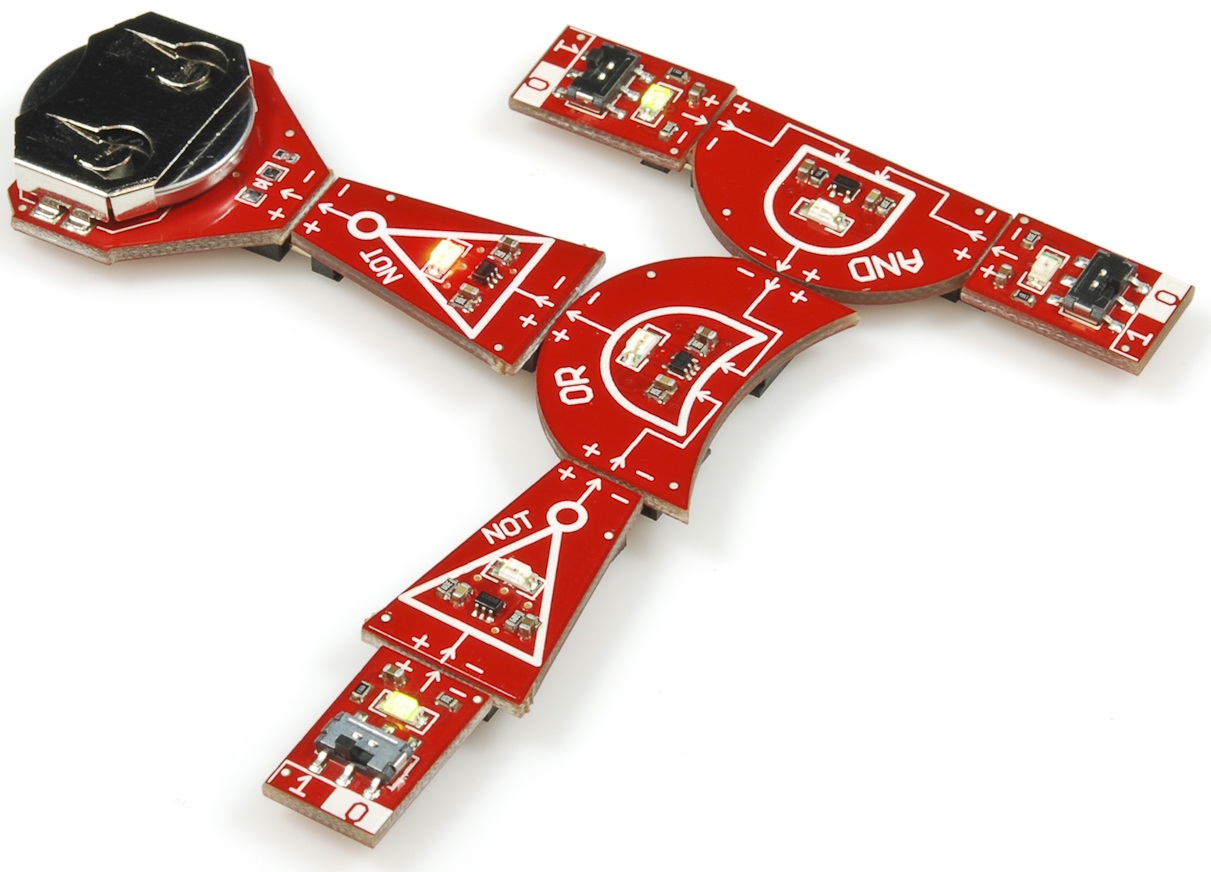
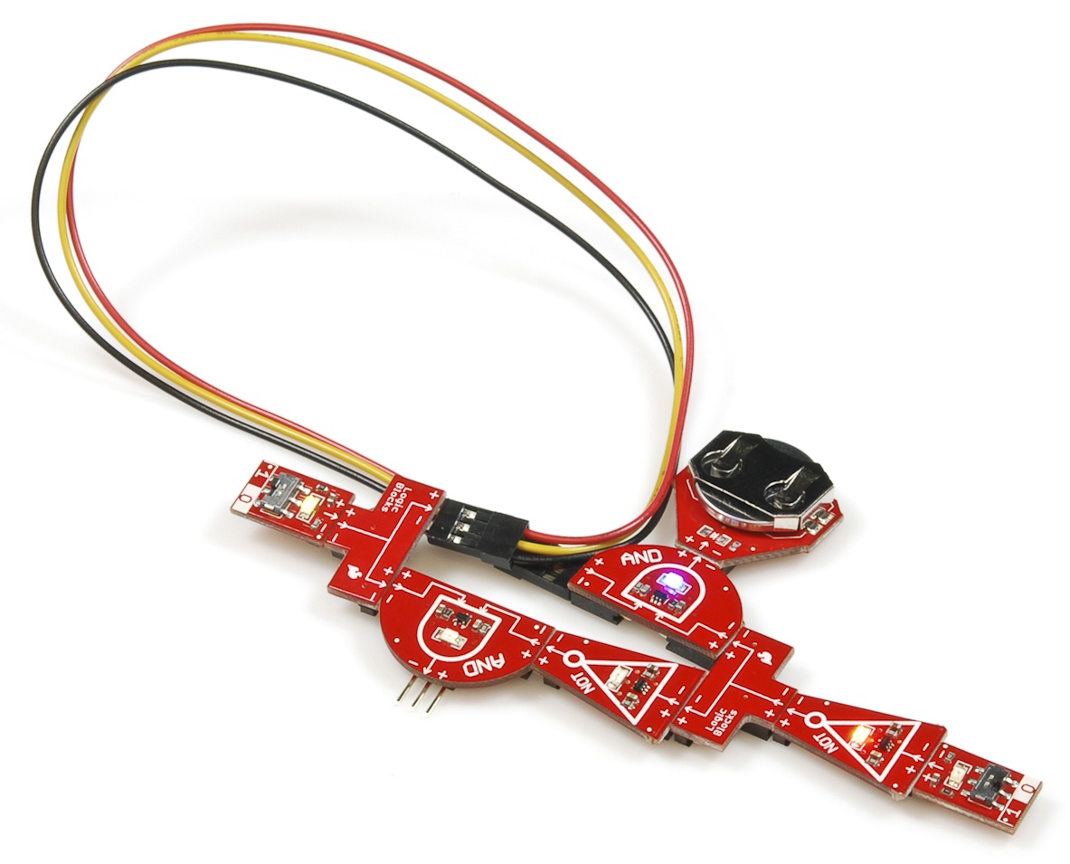
So you've read through the LogicBlocks introductory tutorial (or the kit's included documentation), and are ready for some experiments!? Here's a breakdown of the experiments we'll be exploring in this guide:
- 2-Input AND Gate
- 3-Input AND Gate
- NANDs, NORs, and De Morgan's Laws
- Combinational Logic
- Ring Oscillator
- SR Latch
- 2-to-1 Multiplexer
- 1-to-2 Decoder (De-multiplexer)
- XOR Gate
- Beyond LogicBlocks...
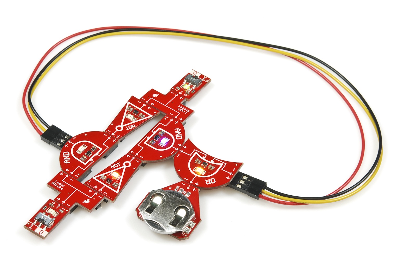
Experiment 1: 2-Input AND Gate
We'll start off as simple as possible: a dual-input, single output AND gate.
What you'll need:
- 1 AND Block
- 2 Input Blocks
- 1 Power Block
Circuit diagram:
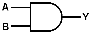
LogicBlock Layout:
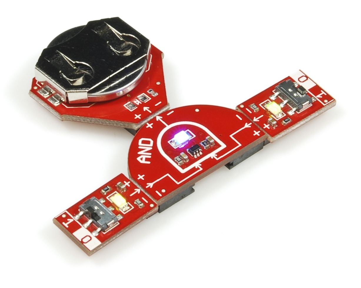
Nothing too fancy here. An Input Block should be inserted into each of the AND Block's inputs. Then plug the Power Block into the output of the AND Block.
The blue LED on the AND Block will indicate the output status of the circuit.
The Experiment:
Try all four possible input combinations: 0/0, 0/1, 1/0, and 1/1. Does the blue AND block LED light up as you'd expect? Remember, this is what the AND gate's truth table should look like:
| Input A | Input B | Output |
| 0 | 0 | 0 |
| 0 | 1 | 0 |
| 1 | 0 | 0 |
| 1 | 1 | 1 |
Sub-experiments:
While we're here, let's discuss the other two fundamental gates:
OR
NOT
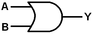
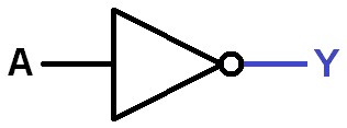
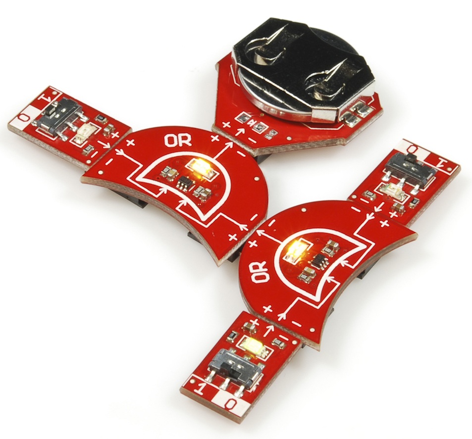
Can you lay out the fundamental OR and NOT gates with LogicBlocks? OR will require a similar set of blocks, while NOT will require just a single input.
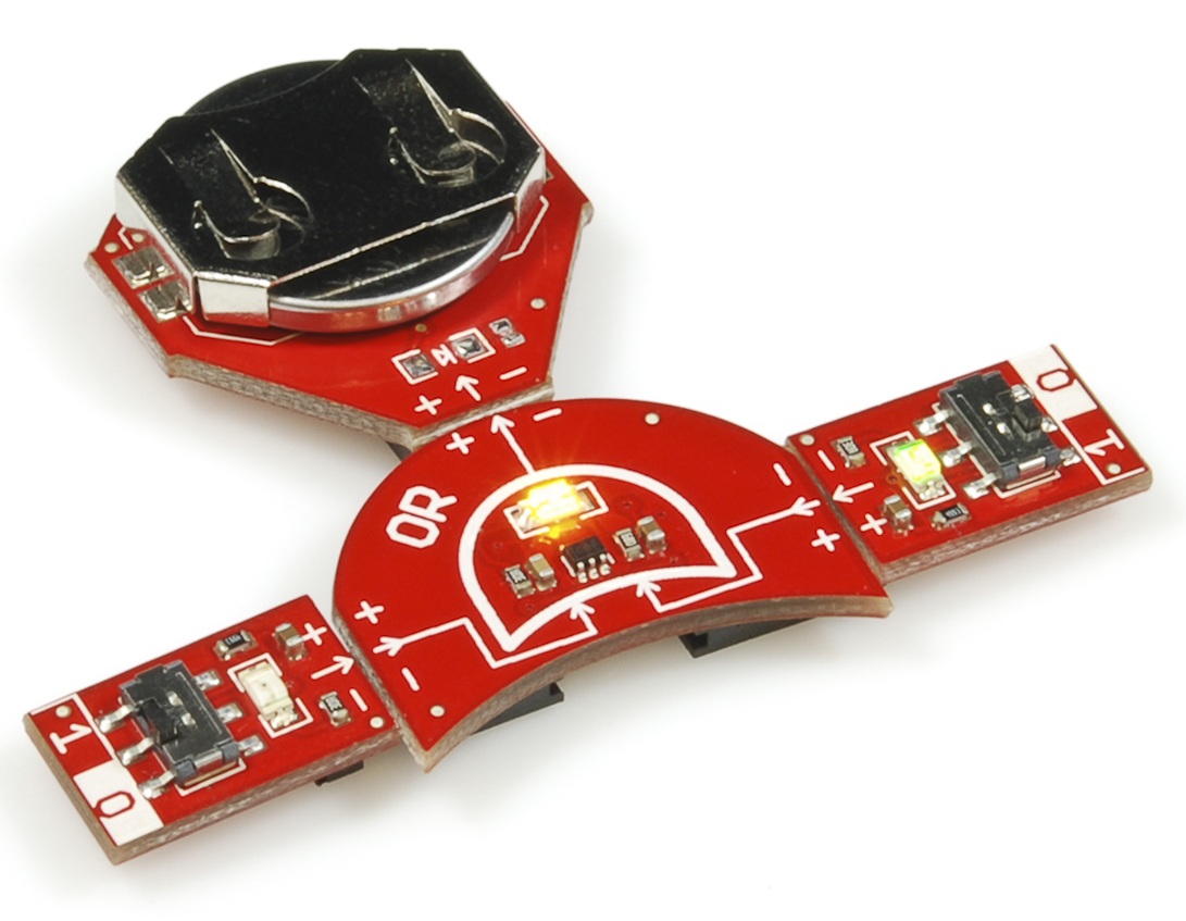
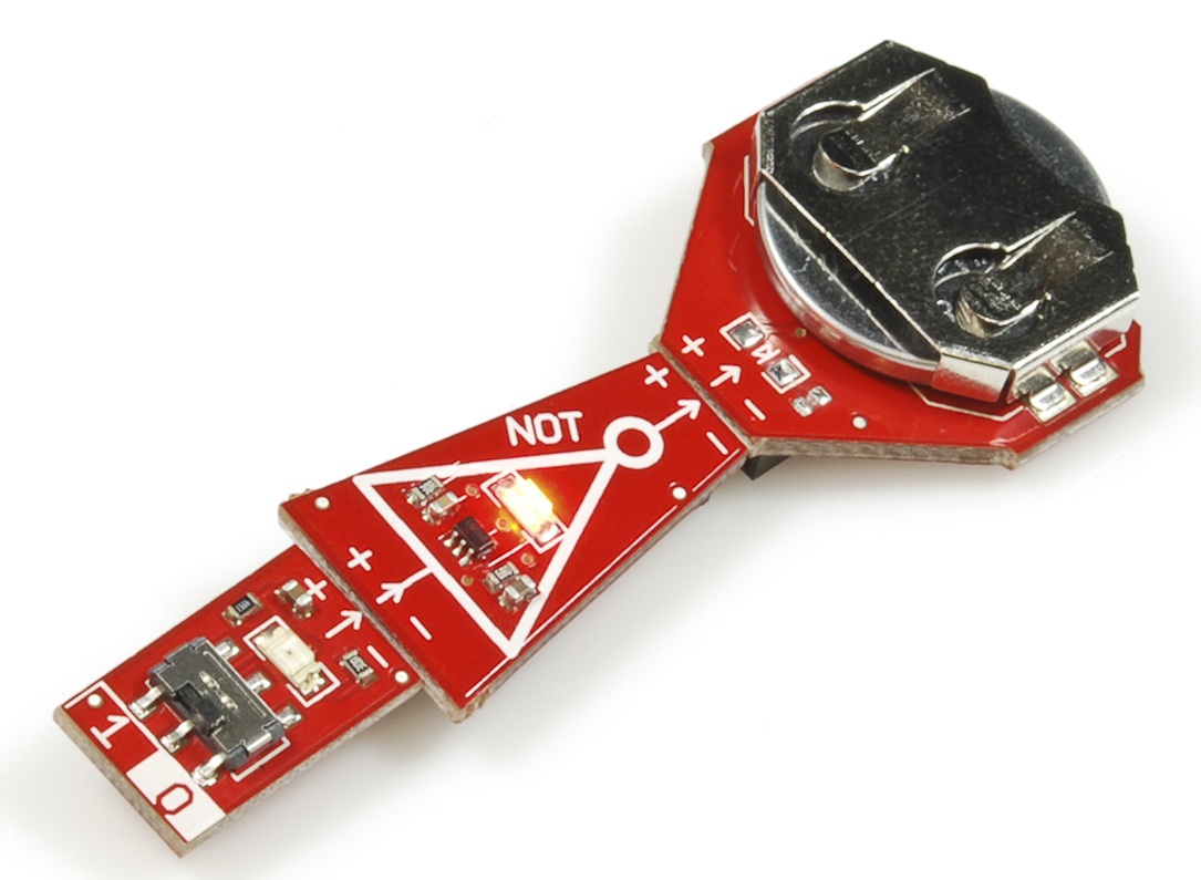
A 2-input OR gate (left) and a single NOT gate (right)
After experimenting with both circuits, fill out their truth tables:
| Input A | Input B | Output |
| 0 | 0 | |
| 0 | 1 | |
| 1 | 0 | |
| 1 | 1 |
| Input A | Output |
| 0 | |
| 1 |
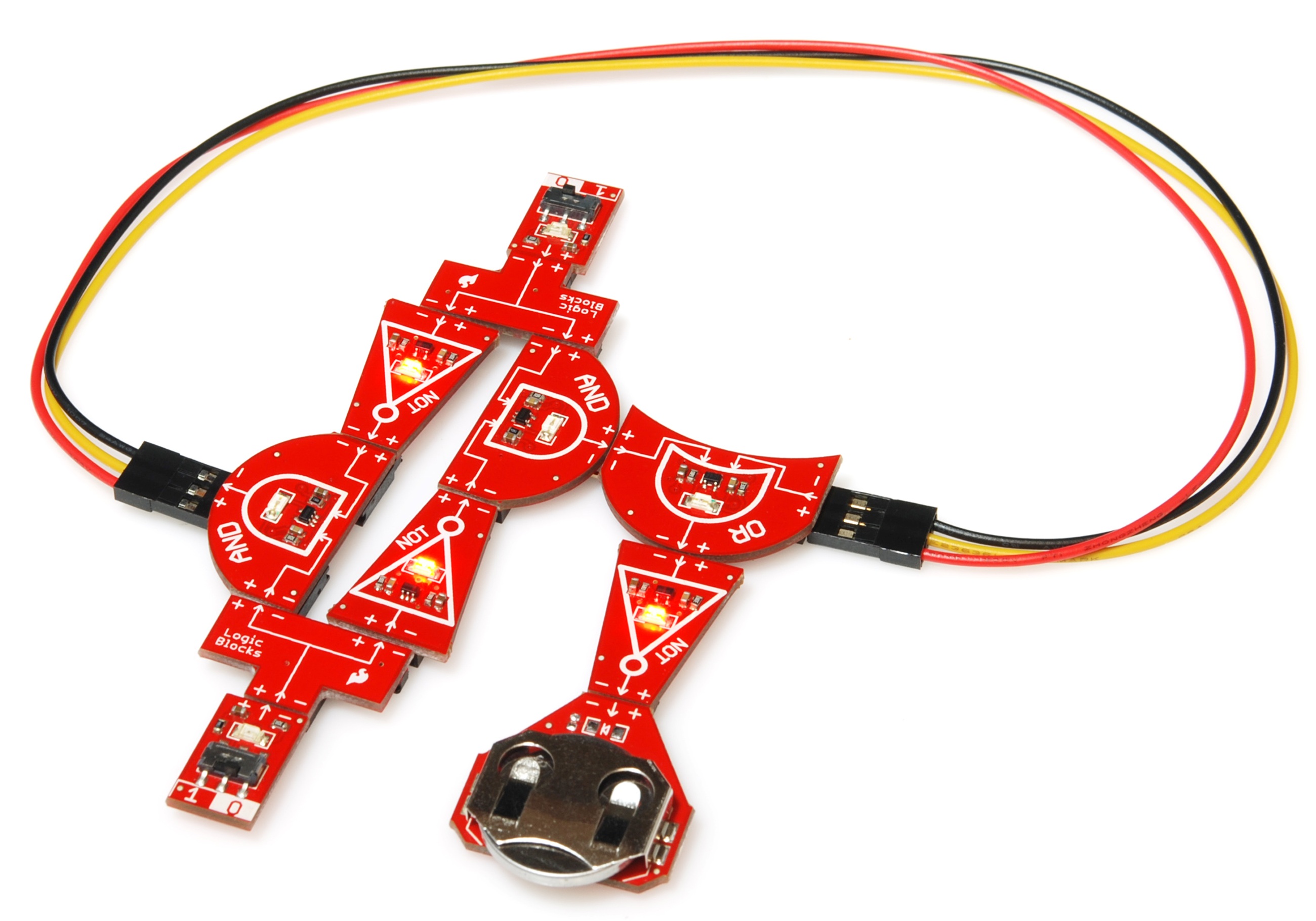
Experiment 2: 3-Input AND Gate
Sometimes you need to AND more than two inputs together. In fact, 3- and 4-input AND gates are as common as the dual-input variety. Let’s make a 3-input AND gate out of two two-input AND gates.
What you'll need:
- 3 Input Blocks
- 2 AND Blocks
- 1 Power Block
Circuit diagram:
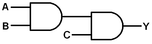
LogicBlock layout:
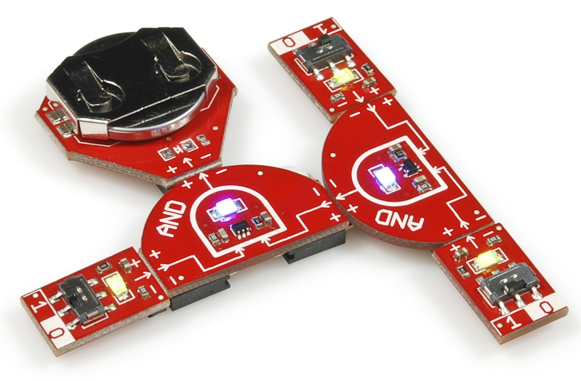
Start by building the 2-input AND block from the last experiment, but plug the output of that AND into the input of another. Then add an Input Block to the second AND's second input. Complete the circuit by adding a Power Block to the output of the second AND.
The blue LED on the second AND gate represents the output of this circuit.
The Experiment:
With three total inputs, how many different input combinations can you make? 8! This number grows exponentially at 2n, where n is the number of inputs. So, a 4-input AND gate has 16 possible combinations, 5-inputs would be 32, and so on.
Try all possible input combinations and fill out the truth table below:
| Input A | Input B | Input C | Output Y |
| 0 | 0 | 0 | |
| 0 | 0 | 1 | |
| 0 | 1 | 0 | |
| 0 | 1 | 1 | |
| 1 | 0 | 0 | |
| 1 | 0 | 1 | |
| 1 | 1 | 0 | |
| 1 | 1 | 1 |
Can you think of a situation in real life where three or more requirements must be met before an outcome becomes true?
If you had more AND blocks, can you imagine what a 4-input AND block might look like?
Sub-experiments:
Try using two OR gates and three Input Blocks to create a 3-input OR gate.
What does the truth table look like for that circuit?:
| Input A | Input B | Input C | Output |
| 0 | 0 | 0 | |
| 0 | 0 | 1 | |
| 0 | 1 | 0 | |
| 0 | 1 | 1 | |
| 1 | 0 | 0 | |
| 1 | 0 | 1 | |
| 1 | 1 | 0 | |
| 1 | 1 | 1 |
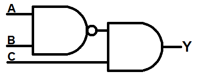
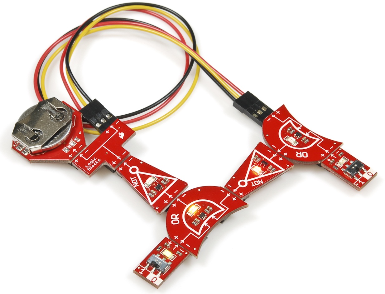
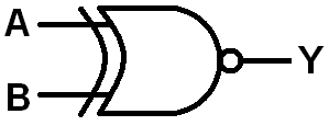
Experiment 3: NANDs, NORs, and De Morgan's Laws
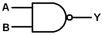
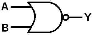
NAND - in other words NOT AND or negated AND - is what you get when you place an inverter at the output of an AND gate. NAND gates are very popular in the world of digital logic. They’ve even got their very own circuit symbol, an AND gate with a “bubble” at the output:
What you'll need:
- 1 AND Block
- 1 NOT Block
- 2 Input Blocks
- 1 Power Block
LogicBlocks Layout:
Similar to the setup from experiment 1, with the addition of a NOT gate between the AND Block output and the Power Block.
The output of this circuit is represented by the red LED on the NOT gate.
The Experiment:
Two inputs...four possible input combinations. Try them all and fill out the 2-input NAND gate's truth table:Can you fill out the truth table for a 2-input NAND gate?
| Input A | Input B | Output Y |
| 0 | 0 | |
| 0 | 1 | |
| 1 | 0 | |
| 1 | 1 |
How does that compare to the truth table of the AND gate?
Sub-experiments:
You can also negate an OR gate to create a NOR:
Which also has its own (bubbled) circuit symbol:
What does the NOR gate's truth table look like?:
| Input A | Input B | Output |
| 0 | 0 | |
| 0 | 1 | |
| 1 | 0 | |
| 1 | 1 |
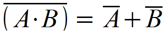
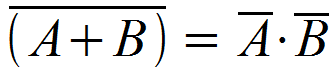
All of this NAND and NOR discussion has me itching to discuss De Morgan's Law! De Morgan's Law allows us to convert NANDs to OR, and NORs to ANDs. There are two parts to De Morgan's Law:
1. A 2-input NAND is equal the OR-ing of two inverted inputs. In boolean equation terms:
2. A 2-input NOR is equal to the AND-ing of the two inverted inputs. Or, in boolean terms:
Prove it yourself! Compare the truth table you filled out for the NAND gate with the truth table for this circuit:
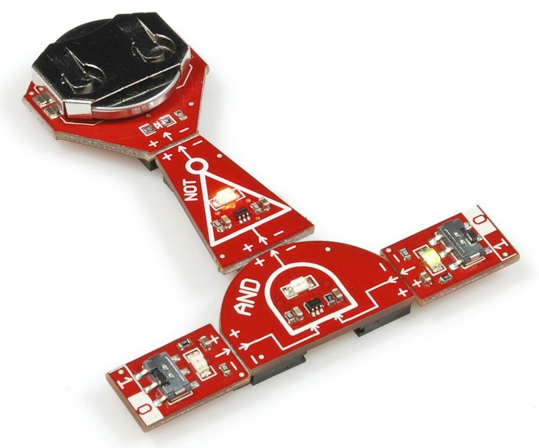
What's the point? Well, a big part of digital logic is simplifying the circuit, and using a few gates as possible. Thanks to De Morgan's Law, we can use a NAND gate to stand in for all of the other gates. For example, a NOT can be made out of a NAND by simply tying one the inputs permanently high:
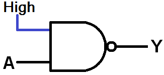
A NOT gate made out of a NAND
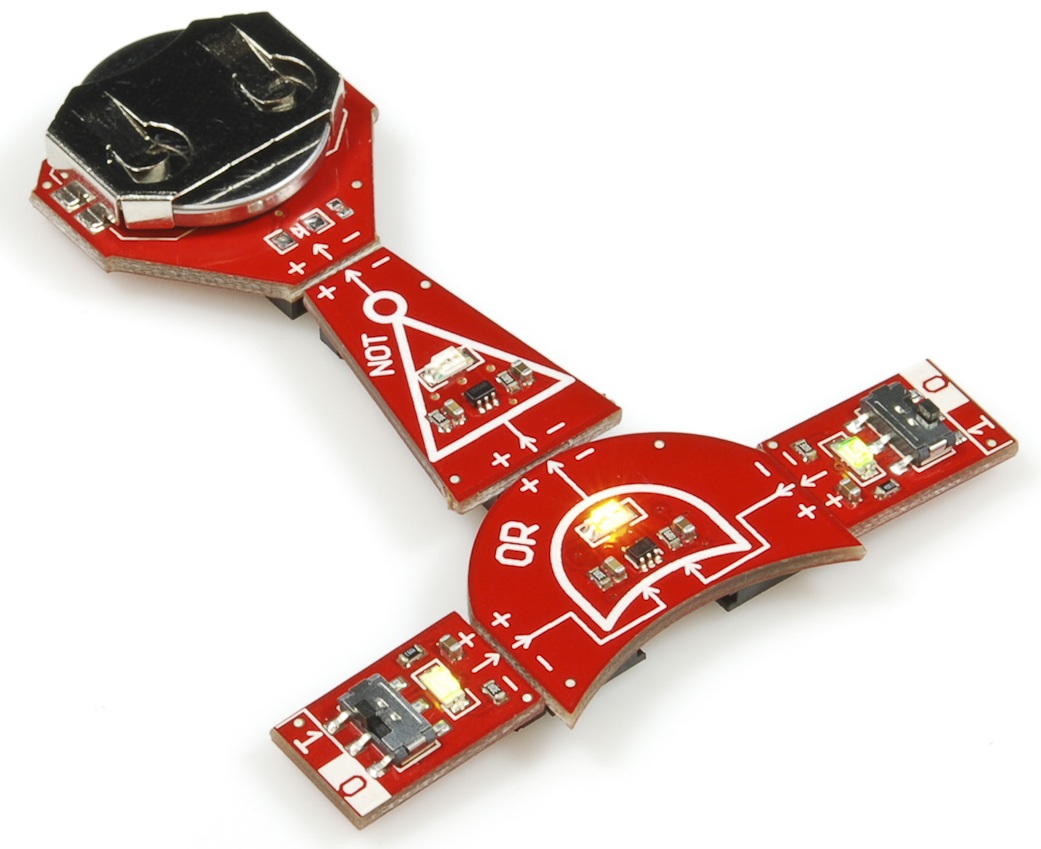
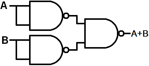
Or use three NAND gates to make an OR:
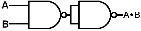
Or use 2 NANDs to make an AND:
NAND gates truly are magical.
Experiment 4: Combinational Logic
The circuits in the previous experiments have all been examples of combinational logic circuits. In combinational circuits the current output depends exclusively on the current state of the inputs. The circuit flows in one direction, from the inputs on the left, to the outputs on the right.
The opposite of combinational logic is sequential, in which a circuits current output will affect its future outputs. But we'll get to that in later experiments.
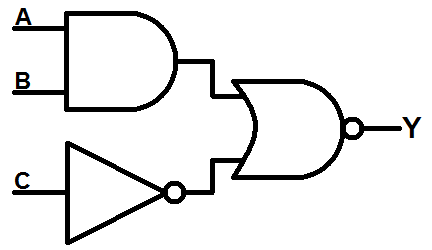
Here's an example of a combinational logic circuit we can build with Logic Blocks:
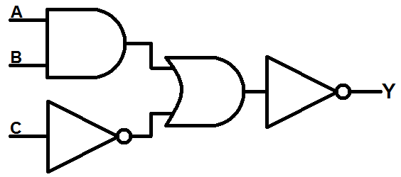
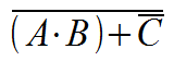
Given the input names shown in the circuit diagram (A and B feeding into the AND gate, C goes through the first NOT gate and so on), we can form a boolean equation like this:
Let's build the above circuit with LogicBlocks.
What you'll need:
- 1 AND Block
- 1 OR Block
- 2 NOT Blocks
- 3 Input Blocks
- 1 Power Block
LogicBlock Layout:
The output of an AND Block, with two Input Blocks connected to the inputs, should be connected to one input of an OR Block. The other input of the OR Block should be connected to a NOT Block, which has an Input Block feeding into it. Finally, the output of the OR Block should feed into another NOT block, which is connected to a Power Block.
The output of this combinational logic circuit is represented by the LED on the final NOT Block.
The experiment:
Try all eight possible input combinations and fill out this circuits truth table:
| Input A | Input B | Input C | Output Y |
| 0 | 0 | 0 | |
| 0 | 0 | 1 | |
| 0 | 1 | 0 | |
| 0 | 1 | 1 | |
| 1 | 0 | 0 | |
| 1 | 0 | 1 | |
| 1 | 1 | 0 | |
| 1 | 1 | 1 |
Does that jive with the equation from above. Have another look at that equation, or even the schematic. Recognizing the NANDs and NORs, could the equation be simplified by using De Morgan's Laws? Yes! First, push that inverter into the OR gate to turn it into a NOR:
Then apply De Morgan's law: push the bubble through the NOR gate - turning that gate into an AND - and through to create NOT gates on both inputs:
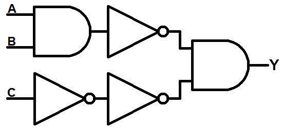
The two NOT gates on the C input would cancel each other out, so just get rid of them both. The NOT gate on the first AND's output can be pushed onto the gate to create a NAND gate:
We've completely eliminated the OR gate! De Morgan's laws could be taken even further - turning the NAND into a NOR with two inverted inputs - but that won't really decrease our gate count. Would you believe that this circuit produces the same truth table as the circuit at the beginning of this experiment? Try it out for yourself:
Sub-experiment:
The next experiment takes a pretty giant leap from combinational to sequential logic. At this point, I'd really encourage you to just play around with the LogicBlocks, create your own circuits. Then try to draw out a circuit diagram, and a truth table.
Are there any real-life scenarios you could imagine solving with digital logic?
Experiment 5: Ring Oscillator
An oscillator is a circuit whose output periodically and repetitively fluctuates. Oscillators are a critical part of most electronic circuits; they're used to create anything from a timer or clock to radio waves and sound.
One of the many oscillating circuits can be created is by connecting together an odd number of NOT gates sequentially, and feeding the output of the last inverter back to the input of the first. This is called a ring oscillator.
What you'll need:
- 3 NOT Blocks
- 1 Splitter Block
- 1 Feedback Cable
- 1 Power Block
Circuit diagram:
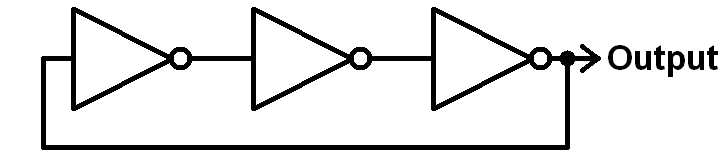
This circuit introduces a concept we've only briefly mentioned so far - sequential circuits. See how the output of third and final NOT gate splits into two directions? The first goes straight out to the output, like we're used to, but it also loops back into the input of the the first NOT gate. This is called feedback - a term almost synonymous with sequential circuits - where the final output of a circuit depends on previous outputs.
LogicBlock Layout:
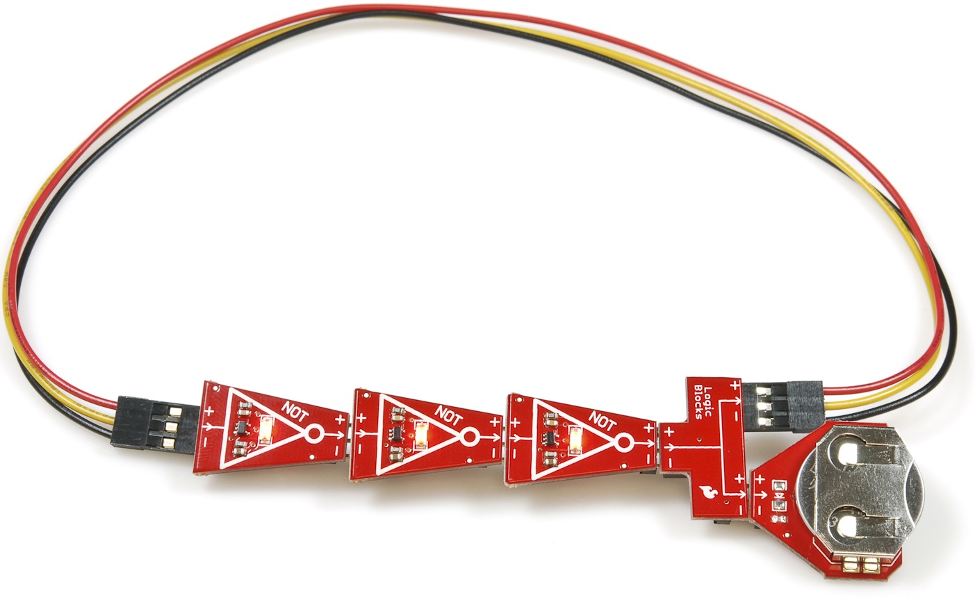
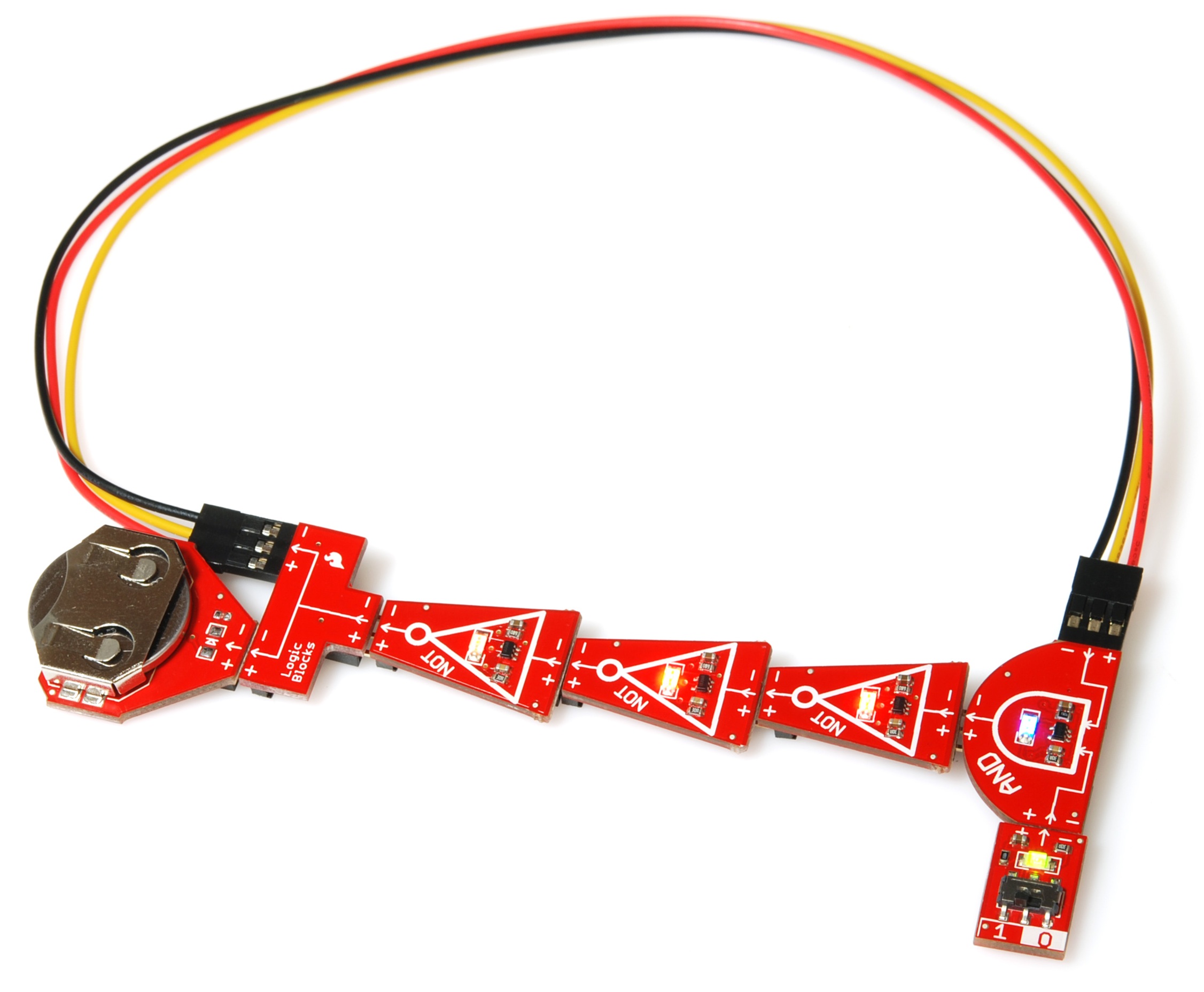
First link up three NOT gates and plug the third's output into a Splitter Block. Use the Feedback Cable to connect one of the Splitter Block outputs to the input of the first NOT gate. Finally, plug the Power Block into the second output of the Splitter Block.
The output of this circuit is represented by the LED on the third and final NOT block.
The Experiment:
What does the truth table look like for this circuit? Wait. Does it even have a truth table?There aren't any inputs. It has something, I'd call it more of a state table:
| Previous Output | Current Output |
| 0 | 1 |
| 1 | 0 |
Does the number of inverters have to be odd? What happens if there are an even number of inverters? Try removing one of them.
Can you calculate how fast the LED on the final NOT Block is blinking? Each block has a delay of about 1 second. What effect would increasing the number of inverters to 5 have on the blinking speed?
Sub-experiment:
In some cases it may be handy to have an enable input on your oscillator. Enable inputs -commonly found in many digital logic circuits - control the overall operation of the circuit. When the enable input is set to 1, the circuit operates as normal, but when its set to 0 the circuit pauses and halts its operation.
We can add an enable input to the ring oscillator by adding an AND gate. Have a look at this circuit diagram:
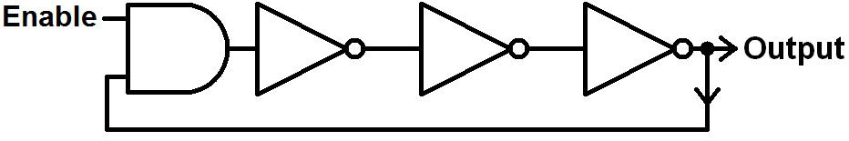
Build it by plugging an AND Block into the first NOT gate (removing the feedback cable). Then plug the male end of the feedback cable into one of the AND Block's inputs, and an Input Block (our enable) into the other input.
Now flip the switch on the enable input to see how it affects the output of the oscillator.
What would the truth table look like now?
| Enable | Previous Output | Current Output |
| 0 | 0 | |
| 0 | 1 | |
| 1 | 0 | |
| 1 | 1 |
Experiment 6: SR Latch
A latch (also called a flip-flop) is a very fundamental form of stable data storage. A single latch can store 1-bit of memory, increase that number by many orders of magnitude and you can create kilo-, mega-, giga-, etc. bytes of storage space. Of course, like most digital circuits, latches are made out of digital logic gates.
There are actually many different kinds of latches, all given somewhat cryptic names like D, JK, and T to name a few. One of the most fundamental latches, though, is the SR-latch, which we can make with a LogicBlocks kit!
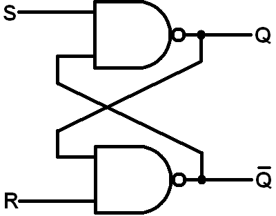
There are a few ways to make an SR latch. Here’s an example of a NOR SR latch:
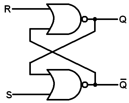
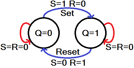
Notice the feedback? This is another sequential logic circuit. Very symmetric too. Two NOR gates each have their output flow into the input of the other. There are two controllable inputs: reset (R) and set (S), which produce the two outputs: Q and Q-not. That's where the SR latch get's its name - it's a set/reset latch.
The SR latch comes with a rule, which cannot ever be broken: the Q-not (Q with the line over it) must always be the opposite of Q (without the line). These outputs are called complements. In truth Q is the only output we really care about - that's where the latch's data is usually stored and retreived - but it's important to observe that the two outputs are opposites.
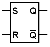
An SR latch is so important it even gets its very own circuit symbol:
The truth table for this circuit is a bit wonky:
| S | R | Previous Q | Current Q | Current Q' |
| 0 | 0 | 0 | 0 (no change) | 1 |
| 0 | 0 | 1 | 1 (no change) | 0 |
| 0 | 1 | 0 | 0 (no change) | 1 |
| 0 | 1 | 1 | 0 | 1 |
| 1 | 0 | 0 | 1 | 0 |
| 1 | 0 | 1 | 1 (no change) | 0 |
| 1 | 1 | 0 | 0 (Restricted, Q and Q' would not be complements) | 0 |
| 1 | 1 | 1 | 0 (Restricted, Q and Q' would not be complements) | 0 |
When S and R are both 0, then Q remains steady, and holds the value it was before. If it was 0 it’ll remain 0, if it was 1 it will still be 1.
Making either S or R 1 is how we set or reset our SR latch.
When both S and R are 1, we enter restricted territory: our rule that Q and Q' must be complements is broken, as they both go to 0. So we call S=1/R=1 a restricted combination. In most latch circuits precautions are taken to keep those inputs from both being 1. Our LogicBlock circuit isn't quite that smart, so you'll need to take the "circuit safety" precautions into your own hands to make sure they're never both 1 (don't worry, the universe should survive the contradiction if you set both inputs high).
All those words, and I probably could have just stuck this state diagram in to explain it for me:
Let's lay out the SR latch with LogicBlocks!
What you'll need:
- 2 OR Blocks
- 2 NOT Blocks
- 2 Input Blocks
- 1 Splitter Block
- 1 Feedback Cable
- 1 Power Block
LogicBlock Layout:
In our mind, we need to assign names to both inputs. One should be R (reset) the other should be S (set). Because the circuit is symmetric, it doesn't matter which input we call which, but the name of the input will affect which output is which.
There are two outputs to keep an eye on in this circuit; both are indicated by the LEDs on the NOT gates. The NOT gate coming out of the OR gate with S as its direct input, indicates the Q' output - the complement. Our Q output is indicated by the red LED on the NOT gate fed by the OR gate with R as its input.
Whew, that all sounds really complicated; refer to the image above, which will do a hundred times better explaining the input/output names and locations.
The Experiment:
Give this series of steps a try, and observe both Q and Q' outputs.
- Begin by setting both S=0 and R=0.
- Now, set R=1. Q should 'reset', if it wasn't already 0, it will become 0. If Q already was 0, it will stay there. Obeying our rule, Q' should be 1.
- Set R=0. Nothing should change on Q or Q'. They hold steady.
- Set S=1. Now Q should 'set' and go high, while Q' goes low.
- Set S=0. There shouldn't be any effect on Q or its complement.
Can you see how this might work as a piece of memory? Imagine a single bit of data being stored in the Q output!
Try entering the restricted state by setting both S and R to 1. Q and Q' should both be 0; our complement rule has been broken! To avoid this from happening safeguards will usually be placed on the inputs (in the form of more logic gates!), which will convert the restricted combination to an allowed input value.
Sub-experiments:
You can also make a latch out of NAND gates. Just swap the ORs with ANDs. Too keep the names of the inputs in line with the outcome they produce, we also swap the S and R inputs (or Q and Q', depending on how you look at it).
And lay it out with Logic Blocks like this:
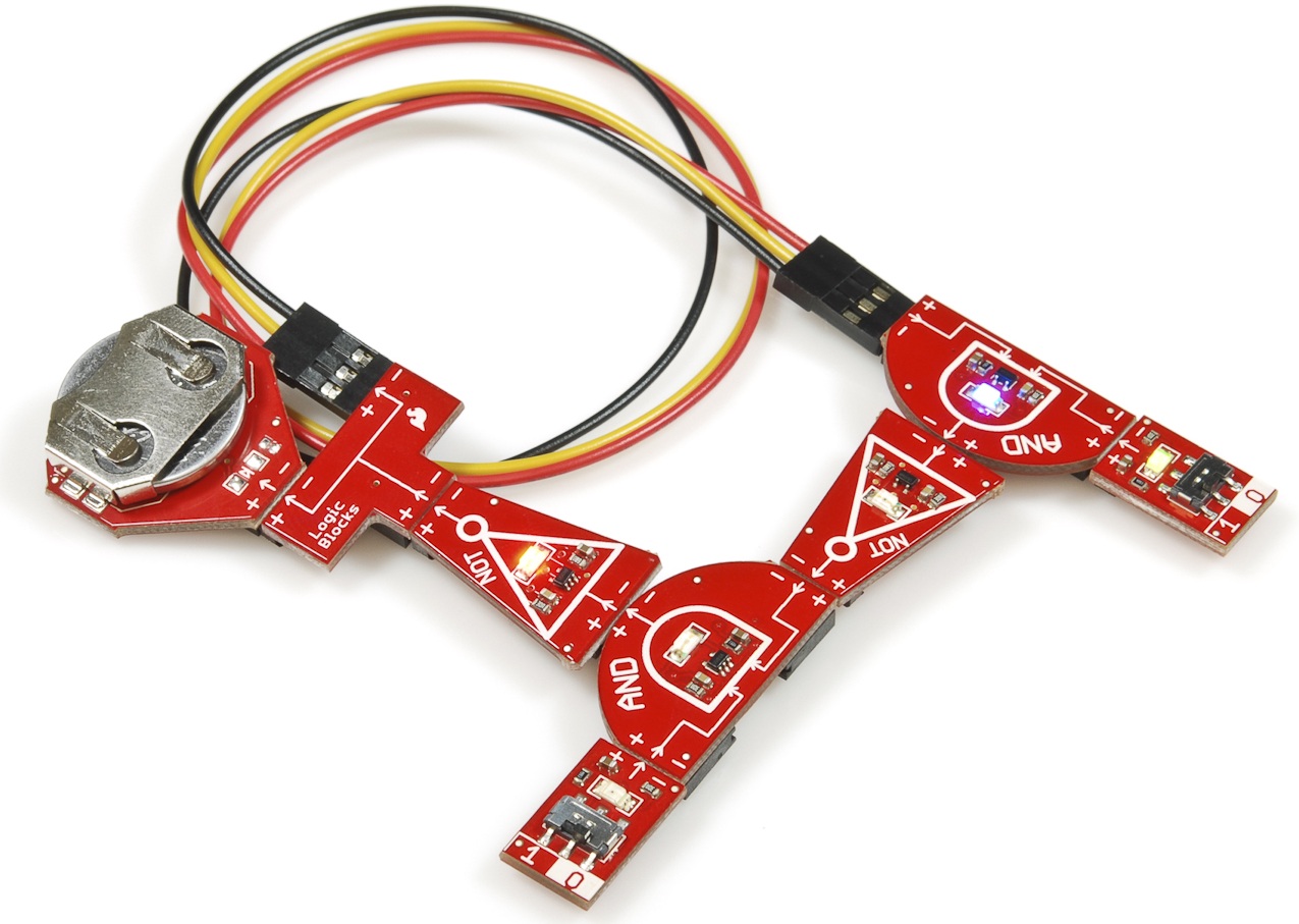
Just replace the OR Blocks with AND blocks!
You still have two stable states, but the truth table changes. Write out the truth table for the NAND SR latch, and compare it with the NOR SR latch above. Which combination of inputs creates a restricted output in this case?
| S | R | Previous Q | Current Q | Current Q' |
| 0 | 0 | 0 | ||
| 0 | 0 | 1 | ||
| 0 | 1 | 0 | ||
| 0 | 1 | 1 | ||
| 1 | 0 | 0 | ||
| 1 | 0 | 1 | ||
| 1 | 1 | 0 | ||
| 1 | 1 | 1 |
Latches are the building blocks of many types of memory, including SRAM (static random access memory). As we've seen, a single latch can store one bit of data. How many latches do you think a piece of 1 Mb (1 million bits) SRAM has? How many NOR gates is that? Zounds!
Experiment 7: 2-to-1 Multiplexer
A multiplexer (or mux) is a common digital circuit used to turn a lot if signals into just one. If you want multiple sources of data to share a single, common data line, you’d use a multiplexer to run them into that line. Multiplexers come in all sorts of shapes and sizes, but they’re all made out of logic gates.
Every multiplexer has at least one select line, which is used to select which input signal gets relayed to the output. In a 2-to-1 multiplexer, there’s just one select line. More inputs means more select lines: a 4-to-1 multiplexer would have 2 select lines, an 8-to-1 has 3, and so on (2n inputs requires n select lines).
Think of a mux as a digital switch. The select line is the throw on the switch, it chooses which of the many inputs get to be the output.
Here’s how you might make a 2-to-1 multiplexer out of logic gates. A and B are the two inputs, X is the select input, and Y is the output.
Here's what a truth table would look like for such a circuit:
| Select Input (X) | Input A | Input B | Output Y |
| 0 | 0 | 0 | 0 |
| 0 | 0 | 1 | 0 |
| 0 | 1 | 0 | 1 |
| 0 | 1 | 1 | 1 |
| 1 | 0 | 0 | 0 |
| 1 | 0 | 1 | 1 |
| 1 | 1 | 0 | 0 |
| 1 | 1 | 1 | 1 |
What you'll need:
- 2 AND Blocks
- 1 OR Block
- 1 Inverter Block
- 1 Splitter Block
- 3 Input Blocks
- 1 Feedback Cable
- 1 Power Block
LogicBlocks Layout:
(Hint: pay more attention than I do to matching up the + and - labels!)
Again, we'll need to internally label each of the inputs. The selector input (X) is the one, lonesome input running into the NOT gate which runs into the splitter. The remaining two inputs are our A and B, which you can arbitrarily name as you wish.
The output of this multiplexer is indicated by the yellow LED on the lone OR gate.
The Experiment:
Give this order of operations a try:
- Start with all three inputs at 0. The output should be 0.
- Flip A to 1. Nothing should happen to the output, because, with the selector switch set to 0, only the B input is being fed into the output.
- Toggle the B input to 1. Observe the output, and set B back to 0. The output should follow your toggling on B!
- With the selector switch set to 1, the output should now follow the A input. The output won't care what B is set to, it'll just do whatever A does.
Is this circuit combinational or sequential? (Don't let the "Feedback" cable fool you!)
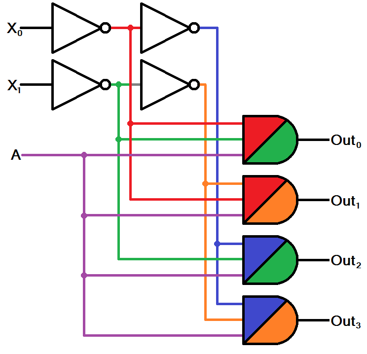
Here's a (color-coded) schematic for a 4-to-1 multiplexer, which requires 4 3-input ANDs, 4 NOTs, and one 4-input OR:
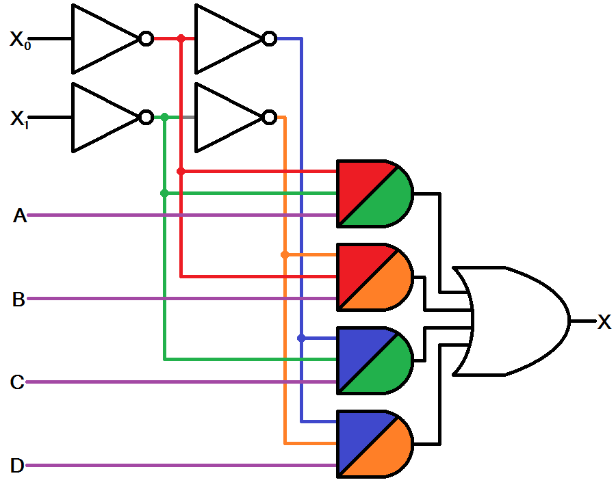
This circuit allows us to choose to send either inputs A, B, C, or D into the X output. X0 and X1 do the selecting.
How many gates do you think a 8-to-1 multiplexer might need?
Experiment 8: 1-to-2 Decoder (Demultiplexer)
The opposite of a multiplexer is a de-multiplexer, also called a decoder. A demux allows a single input line to be passed through to multiple output lines, again using a select line to choose which output the input goes to.
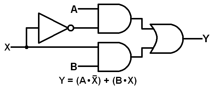
The schematic for a 2-to-1 demultiplexer looks like this:
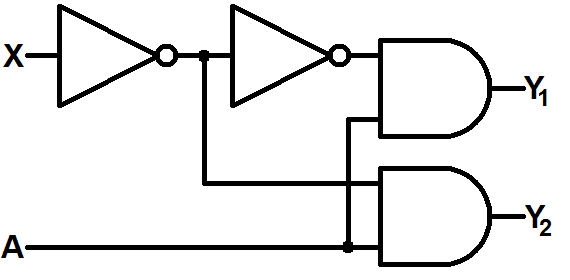
There are two inputs (X and A) and two outputs Y1 and Y2. X is our selector input, it decides which of the two outputs the A input is routed to. When X is 0, the output at Y2 mirrors A (while Y1 will always be 0). Likewise, when X is 1, the A input is routed to Y1.
The demultiplexer becomes really handy when we have limited outputs available in our system and we need to interface with many many input devices.
What you'll need:
- 2 AND Blocks
- 2 NOT Blocks
- 2 Input Blocks
- 2 Splitter Blocks
- 1 Power Block
- 1 Feedback Cable
LogicBlocks Layout:
In this LogicBlock circuit, our selector input (X) is represented by the Input Block that runs into the NOT Block. The only remaining input is our A input.
The two outputs are each represented by the blue LEDs on each of the AND gates. Y1 is the AND Block without the Power Block attached.
The Experiment:
Give this set of operations a try:
- Flip the selector input (X) to 0. Then try toggling the A input both high and low. Only one of the AND Blocks should change, and it should be the same value as the input.
- Then flip the X input to 1. Again toggle A a few times. Now the other AND gate should be keeping pace with A.
Here's a (fancifully colored) circuit for a 2-to-4 decoder:
This circuit has two selector inputs (X0 and X1) which route our input (A) to one of the four outputs.
How does that compare to the 4-to-1 multiplexer circuit? Can you imagine what a circuit for a 3-to-8 decoder might look like?
Experiment 9: XOR
Up till now, you've been happily living in a world with just three fundamental logic gates. I'm going to shatter that world. Prepare for the revelation that is...the exclusive OR.
An exclusive OR, shortened to XOR, is similar to an OR gate with one major difference. Can you tell from the truth table?:
| Input A | Input B | Output |
| 0 | 0 | 0 |
| 0 | 1 | 1 |
| 1 | 0 | 1 |
| 1 | 1 | 0 |
When we say exclusive, we mean it. An XOR only produces a 1 when a lone input is also high. If two or more inputs are 1, the XOR gate outputs a 0.
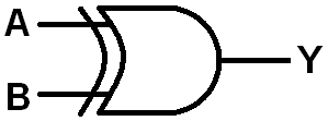
It turns out the XOR gate is an incredibly useful logic function in digital logic. So useful, in fact, that it gets its own circuit symbol. Kind of a modified OR gate, with a concave line preceding the gate we're used to:
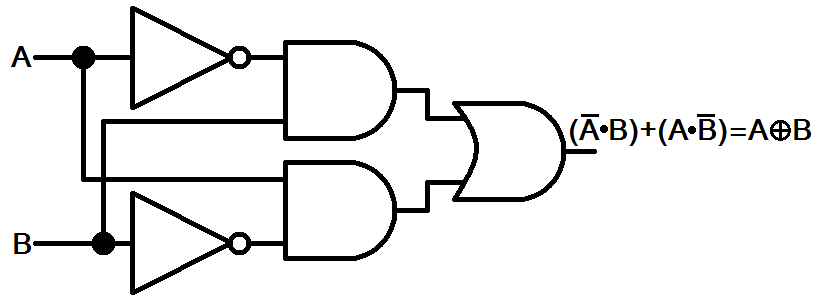
Like all of the previous experiments, the XOR gate can be implemented with the three fundamental digital logic gates. A mix of NOTs, ANDs, and an OR:
Let's LogicBlock it!
What you'll need:
- 2 AND Blocks
- 1 OR Block
- 2 NOT Blocks
- 2 Input Blocks
- 2 Splitter Blocks
- 1 Power Block
- 1 Feedback cable
LogicBlocks Layout:
The output of the XOR LogicBlocks circuit is represented by the yellow LED on the final OR gate.
The Experiment:
Prove the XOR truth table true by toggling both inputs. The LED on the OR block should only light up when you have one or the other of the inputs on.
Is the XOR a combinational or sequential circuit?
Can you think of a real life example where a statement is true if only one of the inputs is also true?
Sub-experiments:
Remember NAND and NOR? Well XOR has it's own complement...XNOR. Like the other two negative gates, XNOR has its own bubbled circuit diagram:
The truth table for the 2-input XNOR looks like this:
| Input A | Input B | Output Y |
| 0 | 0 | 1 |
| 0 | 1 | 0 |
| 1 | 0 | 0 |
| 1 | 1 | 1 |
What's really neat about the XNOR is it only proves true when both inputs are the same. That's why we call this operator the logical equality. You could even use the equals sign (=) as the XNOR operator. Obviously, this equality operator is used all over electronics and programming. If you ever need to check if two statements are equal, you'll use an XNOR.
Hey we've got another NOT Block lying around, let's make an XNOR LogicBlocks circuit. Replace the Power Block with a NOT Block, and plug the Power Block into the end of that.
The output of this circuit is represented by the LED on the final NOT Block.
Now try toggling both Input Blocks. Does the output LED only illuminate when they're both equal?
...Back to top...
Beyond LogicBlocks...
So far we've really just covered the tip of the proverbial iceberg. I hope you can begin to envision just how deeply rooted digital logic is into electronics, but there are so many fundamental digital logic circuits I'd love to cover. Unfortunately, I've run out of blocks. Here are a few of the foundational circuits and concepts I'd be remiss if I didn't discuss:
Adders
Not the snakes...actual circuits that add numbers. Built from digital logic of course! The most basic adder, a half-adder, just adds two bits together, and has two outputs: the sum (S) and a carry (C). And the circuit is actually pretty simple:
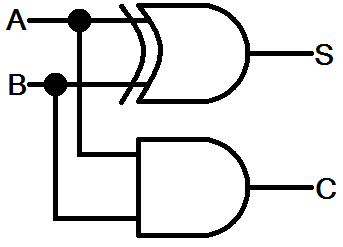
The sum of the two bits is just their XOR, and if both A and B are 1 we generate a carry output.
More complete adders, called full-adders, also have a carry input. These circuits can be strung together in long chains to create a multi-bit binary adder.
Most processors have a block of circuitry within them called an arithmetic logic unit (ALU), where all of the addition, subtraction, multiplication, and division operations are performed. Here hundreds of adder circuits (among others) are housed, and linked to create enormous 32- or 64-bit adders.
Flip Flops (Latches)
We talked about flip-flops in the SR Latch experiment, but I don't think I explained just how important these circuits are. The SR flip-flop we made is one of the more simple latches in electronics.
We can modify the SR latch to create a D latch:
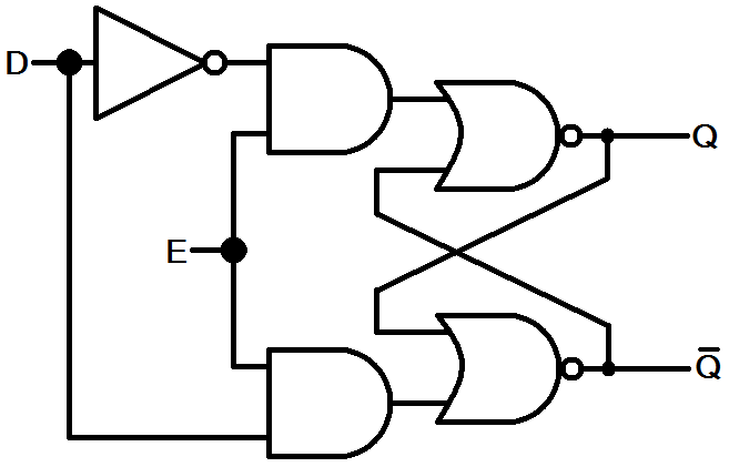
Notice the SR latch in there? The D latch has two inputs - data (D) and enable (E). As long as the enable input is 1, the Q output will be whatever D is. If enable goes low, Q will retain its set value regardless of what the data input does.
Another of the more popular latches is the JK latch. This latch is also based on the SR latch, but it modifies that "illegal" set of inputs (the one where Q and Q' were equal) to instead toggle the current output. Here's how the JK latch is built:
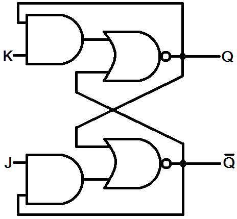
The truth table for a JK latch looks something like this:
| J | K | Previous Q | Current Q |
| 0 | 0 | 0 | 0 (hold state) |
| 0 | 0 | 1 | 1 (hold state) |
| 0 | 1 | X (Don't care) | 0 (reset) |
| 1 | 0 | X | 1 (set) |
| 1 | 1 | 0 | 1 (toggle) |
| 1 | 1 | 1 | 0 (toggle) |
Now, let's turn that JK latch into a JK flip-flop. Flip-flops are usually created by adding a clock input to a latch. A flip-flop with a clock input will usually only perform an operation on the rising edge of a clock signal. The clock input can be used in many ways, for instance multiple flip flops can be synchronized by sharing a clock input. By replacing those 2-input AND gates with a 3-input variety, we can add a clock input to the JK flip-flop:
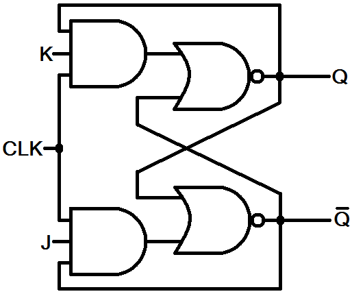
Now, the JK flop-flop will only produce a new output when the clock input is high. This gives us a bit more control over the operation of the flip-flop.
The JK flip-flop will come in handy in the next section...counters.
Counters
Adders add and counters count. Counters are a key element in most processors, especially in timing applications. That digital clock has to count seconds somehow, right?
A really simple counter can be created by linking together numerous JK flip-flops. If multiple JK flip-flops are all set to constantly toggle (J=K=1), and we link the output of one flip-flop to the input of the next, we can create an asynchronous ripple counter. Here's how we might make a 3-bit ripple counter out of JK flip-flops:
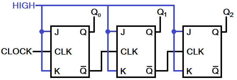
Q0, Q1, and Q2 are our three outputs; Q0 the least-significant bit, Q2 most. With three bits, this circuit can count all the way from 0 to 7 in binary. We can apply a periodic clock to the initial clock input, and begin the counting. Every rising edge on the clock leads to an increment on the counter. Since we've hooked up the complemented output from one JK to the clock input of the next, the Q outputs will toggle whenever the previous one falls.
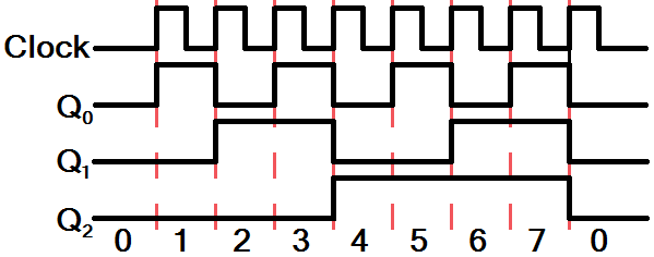
This 3-bit counter will overflow at 7, but adding more flip-flops will increase the upper limit by powers of 2 (n flip-flops count to 2n-1), so we'd need 20 flip-flops to count above 1 million.
There are many other types of counters, but this is a good foundational example built with logic circuits that aren't actually all that far of a stretch from what we've learned so far.
7400 Series Logic Chips
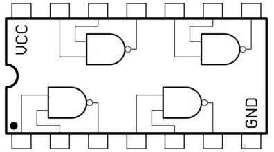
If you're looking for somewhere to go after LogicBlocks, I'd recommend looking into 7400 series logic chips. The 7400s are a huge range of ICs (integrated circuits) that implement all sorts of digital logic functions. You can find quad-NAND gates, along with a variety of other standard digital logic gates. In fact, the chips on the LogicBlock Gate blocks are 7400-series parts - little single-circuit SMD versions.
There are also flip flops, counters, multiplexers, decoders, all sorts of stuff that we've covered in this tutorial is implemented in a 7400 series chip. Even more complicated circuits like entire 4-bit ALUs, memories, comparators...seriously, it's a pretty long list,check this out.
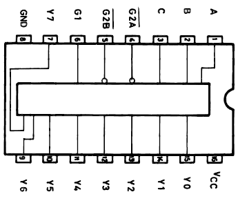
Most 7400 series chips come in a breadboard friendly DIP package, like the 3-to-8 decoder below (74238). So you can experiment and explore without having to actually solder anything.
If you still can't get enough digital logic, CPLDs (compact programmable logic devices) or even FPGAs (field programmable gate array) would be the next step. They represent a giant leap in complexity from even the 7400 series chips, but those ICs can pack thousands of configurable digital logic circuits into a tiny space. There's a lot of digital logic out there for you to explore, but I hope the LogicBlocks have been a good introduction.
Thanks for reading! If you've got any questions about LogicBlocks, or digital logic in general, please post away in the comments below!
0 comments:
Post a Comment